Peng Xin, reporter for 21st Century Business Herald
Intel The first 18A process chip has been unveiled. (January 5, 2026, local time, Las Vegas, USA, Consumer Electronics...) During CES, Intel officially released its third-generation Core Ultra processors, codenamed "Panther Lake." These chips are manufactured using Intel's 18A process and represent Intel's most advanced semiconductor technology . Manufacturing process.
"Intel has delivered on its promise to ship chips manufactured using the 18A process by 2025. In fact, we achieved our goal ahead of schedule," Intel CEO Lip-Bu Tan said at the start of the launch event. He added that the third-generation Core Ultra processors were already in production and being delivered in excess by the end of 2025.
Chen Liwu emphasized that only Intel possesses the unique ability to tightly integrate chip design, advanced processes, and packaging technologies, and that the new generation of Core Ultra processors is designed for an AI-driven future.
18A refers to the 1.8-nanometer process. In the chip industry, a smaller process node in nanometers generally means stronger performance and lower power consumption. This means it is comparable to TSMC. The N2 manufacturing process is roughly equivalent. Before the 14nm node, Intel had long held a lead over major foundries such as TSMC and Samsung in process technology. However, when switching to the 10nm process, Intel encountered bottlenecks and gradually lost its leading advantage.
Previously, Intel's second-generation Core Ultra processor, codenamed "Lunar Lake," raised questions about its chip manufacturing capabilities because it primarily outsourced the core computing modules to TSMC . This new generation of Core Ultra processors signifies the "return" of Intel's core manufacturing capabilities.
Jim Johnson, Intel's Senior Vice President and General Manager of the Client Computing Group, explained that the third-generation Core Ultra processors feature a discrete modular architecture, a larger GPU than any other in its class, and further optimized power consumption. Compared to the previous generation, the new generation of Core Ultra processors offers up to 60% better overall performance.
The new generation of Intel Core Ultra processors covers applications ranging from mainstream thin and light laptops to high-performance mobile workstations. Flagship models are equipped with up to 16 CPU cores, an NPU (Neural Processing Unit) with 50 TOPS of computing power, enhanced graphics capabilities, and support for the latest connectivity technologies, including high-bandwidth memory. It has been optimized to meet the data throughput requirements of AI applications.
Intel announced that the first consumer laptops equipped with third-generation Intel Core Ultra processors will be available for pre-order on January 6, 2026, and will be available globally starting January 27, 2026.
At the launch event, Intel revealed plans to leverage the Panther Lake design to launch products for handheld gaming. A dedicated platform for handheld gaming. In recent years, the handheld gaming market, driven by Valve's Steam Deck, has grown rapidly; this sector was previously dominated by AMD's APU product line. Meanwhile, there are also applications in industry, healthcare, and smart cities. For scenarios such as [specific scenarios not specified], the third-generation Core Ultra edge processor version was released simultaneously with the PC version for the first time. Intel stated that this product series has received embedded and industrial-grade certifications and is expected to be available in the second quarter of 2026.
The mass production and launch of the first 18A process chip is of great significance to Intel. The market generally believes that this product will be key to verifying the quality of the 18A process, and its performance will directly reflect whether Intel can maintain its footing in the competition with AMD. More importantly, it will verify whether Intel has the ability to narrow the gap with TSMC in the field of advanced process technology, or even challenge the latter's dominant position.
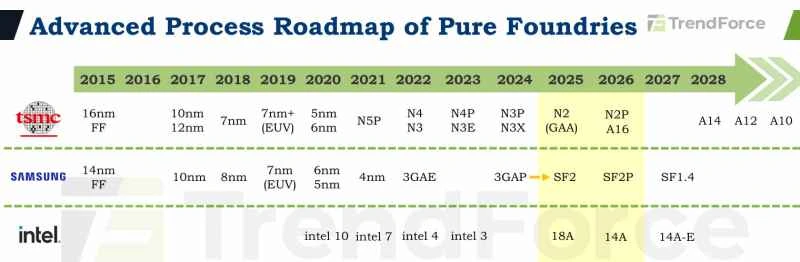
(TSMC, Samsung, and Intel's advanced process node layout. Image source: TrendForce)
The global competition for advanced semiconductor manufacturing processes has advanced to the 2nm mark, leaving only TSMC, Samsung, and Intel as the three major players. A TrendForce report indicates that the technological iteration of these three giants will accelerate further this year: TSMC, after entering the 2nm stage at the end of last year, will evolve towards N2P and A16 processes this year; Samsung plans to upgrade its SF2 to SF2P; and Intel, while implementing its 18A process, has already begun its push towards the next-generation 14A node.
During the tenure of former Intel CEO Pat Gelsinger, Intel continuously strengthened its chip manufacturing capabilities. In July 2021, Intel announced a plan to evolve five new process nodes within four years, culminating in the launch of its 18A process in 2025, regaining its leading position in the industry. During this period, Intel established its Foundry Business Unit (IFS) and invested heavily in building manufacturing facilities.
Intel had high hopes for its 18A process technology and actively sought out foundry customers. In February 2024, Intel announced that Microsoft... One of the designed chips will be manufactured using the 18A process; in September of the same year, Intel announced an expansion of its cooperation with cloud computing... Manufacturer Amazon In a collaboration with AWS, Intel's foundries will manufacture AI chips for Amazon AWS using the 18A process. And manufacturing server chips for Amazon AWS on Intel's 3nm process. There are also rumors that AMD and Apple... They may consider having Intel manufacture some of their chips.
However, in March 2025, after Chen Liwu took the helm at Intel, he launched a series of sweeping reforms, including cost-cutting, promoting a flatter organizational structure, and adjusting the personnel and organizational structure. Chen Liwu discontinued Intel's manufacturing projects in Germany and Poland and announced a further slowdown in the construction of a factory in Ohio, USA. This series of strategic contraction measures cast a shadow over the future of Intel's manufacturing business.
Just as market confidence was wavering, a major deal in September of that year brought a turning point. Nvidia Nvidia announced a $5 billion investment in Intel at $23.28 per share, and the two companies plan to jointly develop AI chips based on the x86 architecture. The market had anticipated that Nvidia's investment would bring Intel more orders and gain the trust of other customers.
Challenges remain. Burdened by historical delays in previous generations of process technology, Intel continues to struggle with yield ramp-up for its 18A process, limiting effective output. This ensures that manufacturing challenges persist. (Wedbush Securities) Wedbush Securities analyst Matt Bryson points out that Intel's transformation will not be achieved overnight.
Matt Bryson believes that Intel still has a lot of groundwork to do, whether it's improving yield rates or implementing the foundry model. Despite short-term setbacks, this doesn't mean Intel's foundry business has limited potential; it simply means the validation cycle will be longer. He further points out that the current 18A node primarily serves Intel's own products, while real external foundry opportunities may focus on the next-generation 14A node.
(Article source: 21st Century Business Herald)